Home > Products > Diamond Lapping Pad

Diamond Lapping Pad

Abrasive type Synthetic diamond
Abrasive grain size 4μm,9μm,20μm
Binder type Resin Bond
Diameter 100mm - 800mm (Compatible with mainstream grinding equipment, customization available)
Thickness 1.5mm - 5.0mm (including adhesive layer)
Get a quote
diamond polishing pad2
diamond grinding pad
diamond polishing pad for wafers
diamond polishing pad2
diamond grinding pad
diamond polishing pad for wafers
Resin Diamond Grinding Pad
Diamond Polishing Pad

Product Overview

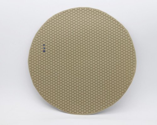
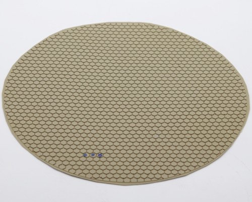
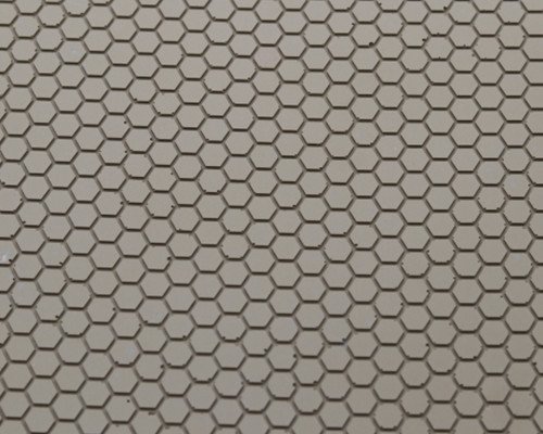
Diamond polishing pads belong to the category of fixed abrasive grinding technology.
Premium diamond micro-powders are firmly bonded within the pad structure, eliminating the need
for slurry mixing. The pads can be directly mounted onto existing lapping or polishing plates
using a pressure-sensitive adhesive backing.

Compared with conventional loose abrasive or CMP processes, diamond polishing pads significantly
improve material removal efficiency, reduce processing time, enhance workshop cleanliness, and
lower overall production and waste treatment costs.

diamond polishing pad2

Key Advantages

  • No slurry mixing required, simplified process flow
  • Fixed abrasive structure ensures stable and efficient material removal
  • Grinding efficiency increased by more than
  • CMP processing time reduced by over 20%
  • Material removal rate up to 2× higher than slurry-based processes with the same grit size
  • Excellent flatness control (TTV, Warp, Bow)
  • Cleaner and more environmentally friendly working environment

Product Features

  • Shallower subsurface damage layer, beneficial for subsequent finishing processes
  • Energy-saving and eco-friendly, no need for wastewater sedimentation systems
  • Lower total production cost compared to loose abrasive grinding

Technical Characteristics

  • High selectivity in the processing area, achieving global planarization with minimal material removal
  • High processing efficiency with reduced power consumption and cycle time
  • Elastic pad structure allows controlled abrasive compliance under grinding pressure
  • Superior surface quality compared to loose abrasives at the same grit size
  • Fixed abrasive particles ensure long service life and high abrasive utilization
  • Pad sharpness can be restored through dressing when dulling occurs
  • Easy post-processing cleaning, ensuring stable surface quality

Specifications of Diamond Polishing Pad

No Grain Thickness
Y 4、9、20um 2.20mm
F 4、9、20um 2.00mm
YF 4、9、20um 2.60mm

Applicable Materials

  • Glass Substrates: Microcrystalline glass, quartz glass, borosilicate glass, float glass, sapphire
  • Semiconductor Wafers: Monocrystalline silicon (Si), silicon carbide (SiC)
  • Functional Materials: Piezoelectric materials such as lithium tantalate (LiTaO₃)
  • Advanced Ceramics: Alumina (Al₂O₃), aluminum nitride (AlN), silicon nitride (Si₃N₄)

Installation

The diamond polishing pad features an adhesive backing design and can be directly mounted
onto existing lapping or polishing plates. Installation and removal are quick and convenient,
with no equipment modification required.

Applications

  • Semiconductor wafer grinding and thinning
  • Glass and optical substrate polishing
  • Advanced ceramic planarization
  • Precision surface finishing of hard and brittle materials

Customization Service

Customized diamond polishing pad solutions are available based on:

  • Workpiece material
  • Target surface roughness and removal rate
  • Machine type and process parameters
  • Pad size, grit size, and hardness requirements

Contact Us

Looking for a high-efficiency, cost-effective, and eco-friendly polishing solution?
Contact us to receive customized diamond polishing pad solutions and technical support.

Diamond Grinding Pad Application Cases

Case 1: Precision Grinding of Sapphire Substrates

Application Requirements: A photoelectric company needed to thin 2-inch sapphire substrates, requiring a TTV (Total Thickness Variation) of ≤5μm, no visible scratches on the surface, improved processing efficiency, and reduced wastewater treatment costs.
Solution: A 30μm grit diamond grinding pad was selected, using a slurry-free grinding process.
Application Results: Grinding efficiency increased by 2.3 times, and CMP (Chemical Mechanical Polishing) time was reduced by 25%; the processed sapphire substrate had a TTV ≤3.2μm, a surface Ra ≤0.008μm, and no subsurface cracks; slurry preparation and wastewater treatment steps were eliminated, reducing single-batch processing costs by 30%.

Case 2: Silicon Carbide (SiC) Wafer Thinning

Application Requirements: A semiconductor chip company needed to thin the back of 6-inch SiC wafers, requiring a stable material removal rate, avoidance of wafer warping, and compatibility with existing grinding equipment.
Solution: A custom-made 400mm diameter, 50μm grit diamond grinding pad was used, directly fitted to the existing grinding disc using adhesive backing.
Application Results: The material removal rate was stable at 8μm/min, and wafer warp was ≤2μm; no equipment modification was required, and installation and debugging time was reduced to 10 minutes per machine; after passivation of the abrasive layer, the sharpness was restored to 95% after trimming, and each grinding pad could process more than 200 wafers.

You may also be interested in
tech@moresuperhard.com
008617700605088