09
Sep
In substrate cutting processes, the properties of different materials directly determine the choice of diamond dicing blades. Proper dicing blade selection not only affects cutting quality but also plays a crucial role in efficiency and cost control. This article introduces blade strategies for three typical substrate materials, along with their common applications, to help optimize decision-making.
Before diving into blade selection, let’s look at where substrates are commonly used:
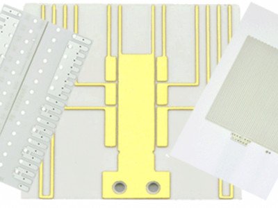
PCB Substrates (FR-4, BT resin): smartphones, computers, automotive electronics, communication devices — the backbone of electronic products.
Metal Substrates (copper, aluminum): high-power LEDs, power modules, and EV control systems, favored for their excellent thermal conductivity.
Ceramic Substrates (Al₂O₃, AlN, Si₃N₄): power semiconductors (IGBT, MOSFET), laser diodes, aerospace electronics, and EV inverter modules.
Silicon / Sapphire Substrates: semiconductor chips, optoelectronics, and LED epitaxy.
These applications demand high precision, minimal damage, and high reliability, making blade selection especially critical.
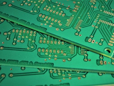
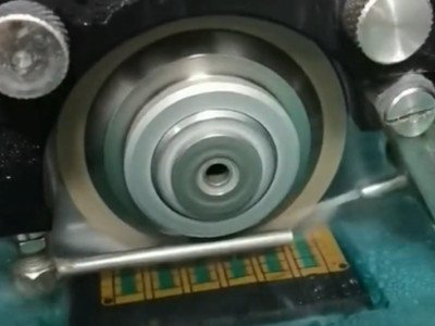
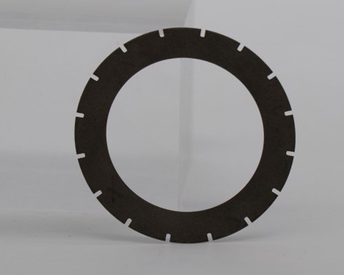
Material characteristics: Contains fiberglass; both hard and brittle, prone to cracks, delamination, and burrs during cutting.
Blade selection:
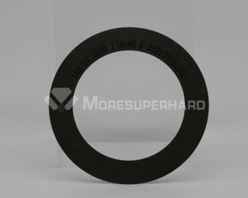
Bond type: Resin bond blades → elastic abrasives reduce impact and edge chipping.
Grit size: #600–#800 for a balance of efficiency and surface finish.
Blade thickness: 0.1–0.3 mm for finer cuts.
Cooling & fixturing: Pure water cooling; standard vacuum chuck.
Typical applications: smartphone motherboards, communication routers, automotive ECUs.
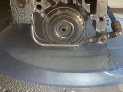
Material characteristics: High ductility, leading to abrasive grain pull-out and chip evacuation difficulties.
Blade selection:
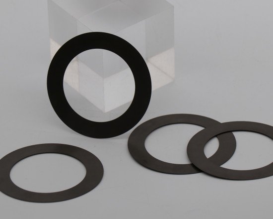
Bond type: Metal bond blades → strong abrasive retention ensures stability.
Coating: SDS coating for better chip removal and heat dissipation.
Grit size: #200–#400 for sharper cutting edges.
Cooling & fixturing: Forced internal cooling with water-based emulsion containing anti-rust agents.
Typical applications: LED lighting boards, power supply modules, EV drive control boards.
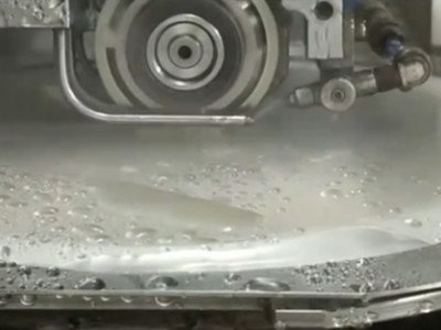
Material characteristics: Extremely brittle and poor thermal conductivity, easily causing edge chipping and heat accumulation.
Blade selection:
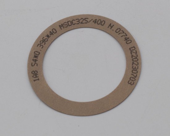
Bond type: Ultra-dense metal bond blades → long tool life and strength.
Grit size: Ultra-fine (#1500–#2000) to achieve excellent surface finish.
Cutting mode: Pulse cutting (intermittent feed) to reduce thermal buildup.
Cooling & fixturing: Deionized water with low-foam additives; polymer chucks to minimize stress concentration.
Typical applications: power semiconductor modules (IGBT, MOSFET), laser diode packaging, aerospace and high-power electronics.
PCB substrates → Resin bond + medium grit (#600–#800) + thin blade edge (0.1–0.3 mm).
Copper substrates → Metal bond + coarse grit (#200–#400) + forced internal cooling.
Ceramic substrates → Ultra-dense metal bond + ultra-fine grit (#1500–#2000) + pulse cutting mode.
By starting from substrate material properties and application scenarios, manufacturers can achieve the best balance of cutting quality, efficiency, and cost, ensuring reliable production for electronics, semiconductors, and optoelectronic industries.