16
Jun
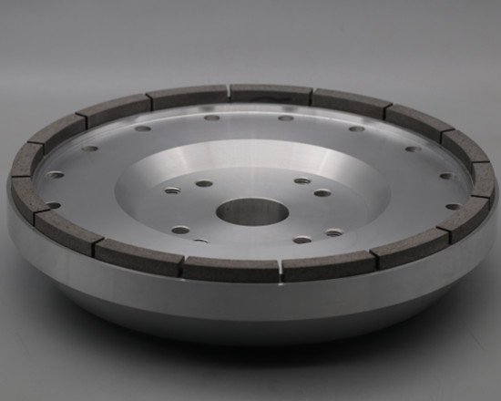
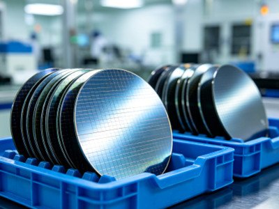
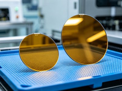
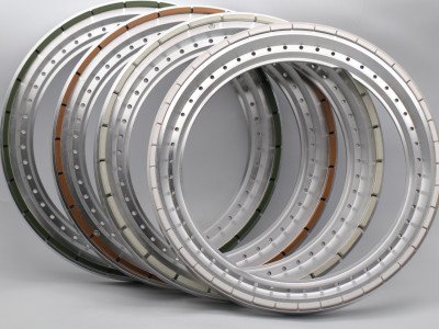
Wafer backside thinning is an indispensable process in semiconductor manufacturing, which directly impacts chip yield, device performance and service life. As the core consumable for this procedure, diamond thinning wheels are specially developed for machining hard and brittle materials such as monocrystalline silicon (Si) and silicon carbide (SiC).
Monocrystalline silicon serves as the fundamental material for traditional integrated circuits, memory chips and IGBTs. Silicon carbide, the core substrate of third-generation semiconductors, empowers new energy vehicles, 5G base stations, photovoltaic energy storage and other high-end industries.
This article elaborates on material characteristics, wheel selection criteria, machining processes and quality control of diamond thinning wheels for Si and SiC wafers. Meanwhile, we introduce professional wafer thinning solutions from Moresuperhard, delivering high-efficiency, low-damage and cost-effective products for global semiconductor manufacturers.

The physical properties of Si and SiC determine the overall selection of grinding wheels and machining parameters.
Mohs hardness: 7, medium brittleness
Original wafer thickness: approx. 775 μm, target thinning thickness: 50–100 μm
Main applications: Logic chips, memory chips, IGBTs and conventional semiconductor devices
Core requirements: High productivity, minimal subsurface damage and low operational cost
Mohs hardness: 9.5 (second only to diamond), extremely high brittleness and thermal conductivity (~490 W/m·K)
Original wafer thickness: approx. 725 μm, target thinning thickness: 50–200 μm
Main applications: Power devices for new energy vehicles, 5G RF components and photovoltaic inverters</p
Core requirements: Crack-free machining, low thermal damage, superior surface finish and precise form accuracy
SiC is far more difficult to machine than silicon, requiring tailored grinding wheels and strict process control throughout production.
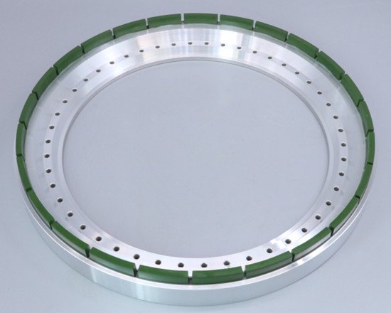
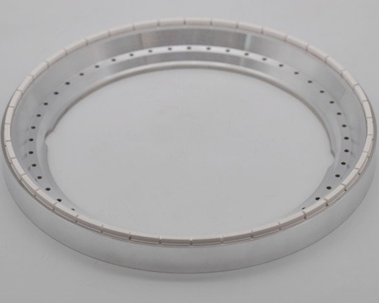
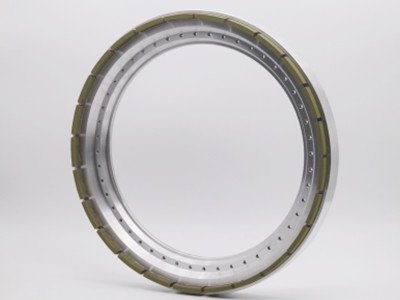
Diamond abrasives are the only choice for efficient machining of ultra-hard SiC materials. The performance of thinning wheels depends on abrasive grain size, bond system, abrasive concentration, porosity and base material.
Grain size distinguishes rough grinding and fine grinding processes, and controls material removal rate and surface quality.
Rough grinding: #1000–#2000, grain size 10–20 μm, Ra 10–20 nm
Fine grinding: #4000–#8000, grain size 2–5 μm, Ra 2–5 nm
Rough grinding: #2000, grain size 8–15 μm, Ra 10–15 nm (to remove residual damage from slicing)
Fine grinding: #8000–#30000, grain size 0.5–2 μm, Ra 0.5–2 nm, TTV < 2 μm. The finished wafers can go directly to polishing.
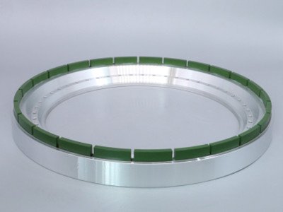
Three mainstream bond types are widely applied in semiconductor thinning wheels, among which vitrified bond is the most popular for domestic and global manufacturers.
Vitrified Bond (Mainstream)
High porosity, excellent self-sharpening performance and moderate thermal conductivity. Suitable for both rough and fine grinding of Si and SiC wafers.
Resin Bond
Good flexibility and outstanding surface finishing effect. Ideal for high-precision fine grinding of SiC wafers, with relatively shorter service life.
Metal Bond
High mechanical strength, long lifespan and superior heat dissipation. Perfect for heavy stock removal in SiC rough grinding and post-packaging machining. Regular dressing is required due to relatively poor self-sharpening.
Abrasive Concentration: 75%–100% for silicon wheels; 100%–150% for SiC wheels (higher concentration for ultra-hard materials).
Porosity: 30%–50%. High porosity ensures efficient chip removal and heat dissipation, effectively reducing thermal damage and cracks.
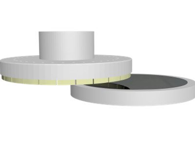
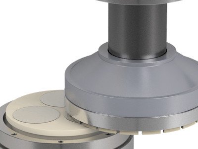
Base Body: Made of aluminum alloy or stainless steel with high rigidity and low vibration. Fully compatible with mainstream thinning machines such as Disco and Tokyo Seimitsu.
Below are mass-production process parameters for 8–12 inch semiconductor wafers.
Applicable equipment: 8–12 inch wafer thinning machines (e.g. Disco DFG800)
SiC is prone to chipping, thermal stress cracks and deep subsurface damage, which calls for stricter process control.
| Index | Monocrystalline Silicon Wafer | Silicon Carbide Wafer |
|---|---|---|
| Surface Roughness (Ra) | < 5 nm (Fine grinding) | < 1 nm (Fine grinding, mirror finish) |
| Total Thickness Variation (TTV) | < 3 μm | < 2 μm |
| Warpage | < 50 μm | < 30 μm |
| Edge Chipping | < 20 μm | < 8 μm |
With years of R&D and manufacturing experience in diamond abrasive tools, Moresuperhard focuses on developing high-performance thinning wheels for Si, SiC and other hard brittle semiconductor materials. We provide one-stop, cost-effective solutions for global clients, covering traditional semiconductors and third-generation semiconductor industries.
Silicon Dedicated Thinning Wheels
Full grain range from #1000 to #8000 with premium vitrified bond. Standard abrasive concentration (75%–100%) and 30%–50% porosity.
SiC Dedicated High-End Thinning Wheels
Including #2000 rough grinding wheels and #8000–#30000 ultra-fine fine grinding wheels, with optional vitrified, resin and metal bonds. Adopt 100%–150% high diamond concentration.
Our products serve wafer manufacturers, third-generation semiconductor component producers, chip packaging & testing factories, new energy electronics and 5G component suppliers worldwide.
Available cooperation modes: Standard products in stock, non-standard customization, trial order and bulk order. Free technical support is provided for trial runs.