10
Oct
In the semiconductor manufacturing process, edge chipping after wafer thinning is a very common and difficult problem. This can lead to a decrease in wafer strength, making it more prone to breakage during subsequent transportation or processing, and directly reducing product yield.

Process Stress: The immense pressure exerted on the wafer edge by the grinding wheel during the rough grinding stage;
Wafer Condition: Inadequate edge treatment, and the original thickness being relatively thin;
Equipment and Fixtures: Uneven vacuum adsorption, insufficient support from the wafer stage;
Operational Steps: Improper handling or contact with the mechanical arm.
1. Process Optimization
Adopt a “two-step” or “three-step” grinding method:
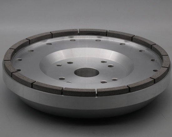
Rough Grinding: Use a coarser grinding wheel to quickly remove most of the material, but control the feed rate to avoid being too aggressive.
Fine Grinding: Switch to a finer diamond grinding wheel and use a smaller feed rate and lower grinding head pressure to remove a small amount of material in a plastic grinding mode. The key in this step is to eliminate the damage layer produced by rough grinding and significantly improve the edge quality.
Reduce feed rate and spindle speed: Appropriate reduction of these parameters can reduce instantaneous stress, although it will slightly increase cycle time, it can greatly improve yield.
Use step grinding: Before grinding to the final thickness, leave a few microns of allowance, and then grind to the final size with fine grinding parameters.
2. Equipment Maintenance and Inspection
Regular dressing and replacement of grinding wheels, inspection and cleaning of the chuck table, and calibration of the robot picker.
3. Enhancing Edge Strength
Optimize edge treatment processes, laser grooving and laser strengthening.
4. Adoption of Advanced Techniques
Temporary bonding, wet/dry etching, and other solutions can almost completely avoid corner chipping problems.
5. Operation Discipline
Train operators, use dedicated thin wafer carriers, and reduce secondary damage.