Home > Products > Polyurethane(PU) Polishing Pad for Optical Lens

Polyurethane(PU) Polishing Pad for Optical Lens

Polyurethane polishing pads are used for thinning and polishing the surfaces of precision materials such as precision optical glass, sapphire, filters, ceramic substrates, quartz glass, disk substrates, laser crystals, silicon wafers, precision metals, watch glass and III-V compound semiconductor materials.
Abrasives Types Alumina, cerium oxide, zirconium oxide and pure polyurethane
Shape Round,Rectangle and other custom shape
Thickness 0.5mm,0.8mm,1.0mm,1.27mm,1.5mm,2.0mm,2.5mmm,3.0mm etc
Applications Applied to the thinning and polishing of the surfaces of precision materials such as precision optical glass, sapphire, filters, ceramic substrates, quartz glass, disk substrates, laser crystals, silicon wafers, precision metals, watch glass and III-V compound semiconductor materials.
Get a quote
Polyurethane polishing pad
polishing pad for silicon wafer
polishing pad for CMP
polishing pad
polishing pad for optical lens
polishing wafer
Polyurethane polishing pad
polishing pad for silicon wafer
polishing pad for CMP
polishing pad
polishing pad for optical lens
polishing wafer
Polyurethane(PU) Polishing Pad for Optical Lens
Polyurethane(PU) Polishing Pad

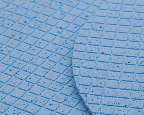
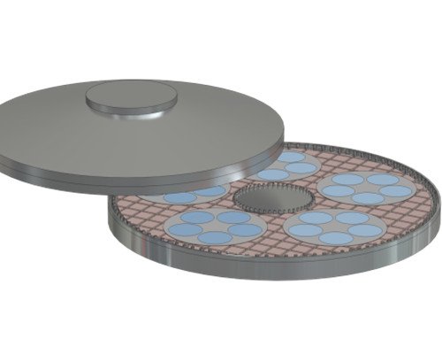
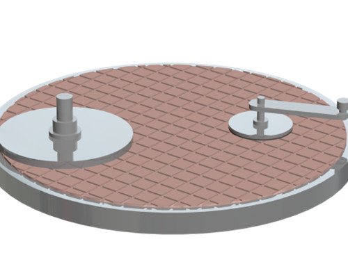
In the manufacturing process of optical lenses, the polishing process is a key step that determines the surface quality. PU (polyurethane) polishing pads, with their unique physical and chemical properties, are widely used in various precision polishing applications, ensuring high efficiency and stable performance in optical processing.

Different PU Material Composition

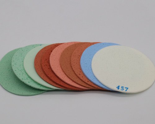
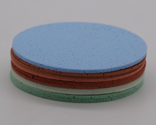
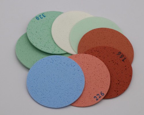
The PU polishing pad is made from specially foamed micro-porous rigid plastic elastomer. Based on the type of abrasive filled, it is classified as:

  • Cerium Oxide Series: Enhances polishing rate
  • Zirconia Series: Improves surface smoothness
  • Alumina Series
  • Pure PU Series: Offers stable pore structure during polishing
  • polishing pad for optical lens

3. PU Pad  Specifications

Shape Dimensions
Rectangle 1397 × 584 mm
1400 × 640 mm
1400 × 700 mm
1500 × 750 mm
1700 × 850 mm
1800 × 900 mm
Circular Φ380 mm
Φ640 mm
Φ960 mm
Φ1050 mm
Φ1200 mm
Φ1300 mm
Φ1350 mm
Thickness 0.5 mm / 0.8 mm / 1.0 mm / 1.27 mm / 1.5 mm / 2.0 mm / 2.5 mm / 3.0 mm

polishing pad for silicon wafer

4.  Features of Moresuperhard PU Polishing Pad

  • Customizable with self-adhesive backing and grooved surface design, ensuring strong polishing power, flatness, and excellent wear resistance.
  • Micro-porous structure ensures effective slurry absorption and controlled material removal.
  • Compatible with various polishing slurries (e.g., cerium oxide, silica) for different materials.

5. Applications

🔬 Optical & Semiconductor Applications

Used for surface thinning and polishing of materials such as:

  • Precision optical glass
  • Sapphire
  • Filters
  • Ceramic substrates
  • Quartz glass
  • Disk substrates
  • Laser crystals
  • Silicon wafers
  • Watch glass
  • III-V compound semiconductors

dressing polishing pad

💼 Industrial Applications

  • Semiconductor Industry: Polishing silicon wafers to improve chip yield
  • Optical Industry: Polishing lenses and optical components
  • Automotive Industry: Polishing engine blocks and crankshafts
  • Jewelry Industry: Polishing jewelry surfaces for enhanced shine

6. Technical Support

We provide customized solutions to meet diverse customer needs, including:

  • Custom dimensions and thickness
  • Grooving patterns
  • Adhesive backing options
  • Material formula adjustments

With the increasing demands for ultra-precision in optical manufacturing, polishing technology is evolving toward greater specialization. Proper selection and standardized use of polishing pads can significantly improve product yield and processing efficiency.

You may also be interested in
tech@moresuperhard.com
008617700605088