04
Nov
QFN is a leadless package widely used in high-density, high-frequency and power-sensitive semiconductor devices. Because it has no protruding leads, the copper leadframe is exposed at the package edge after singulation. During dicing, defects typically appear in three forms:
EMC chipping / peeling — fracture of the brittle epoxy molding compound along the cut edge.
Copper burrs (flash) — ductile tearing of the copper leadframe that leaves burrs on the side wall.
Substrate delamination — separation at the copper-to-EMC interface.
Any of these defects can expose internal circuitry, reduce solder-joint reliability, and cause devices to fail electrical testing — driving down yield and increasing scrap cost in high-volume packaging lines.
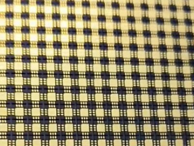
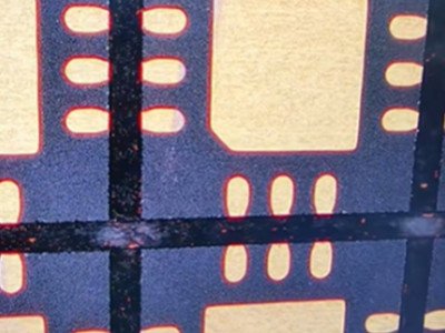
Chipping originates from excessive mechanical impact, thermal stress and unstable cutting conditions at the EMC‑copper boundary. Four dominant contributing factors are summarized below.
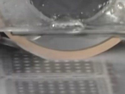
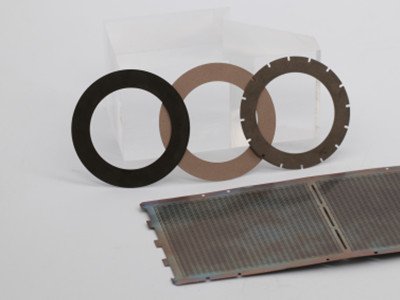
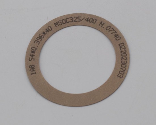
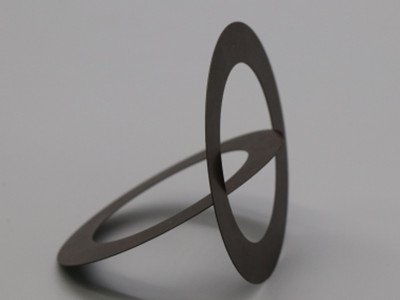
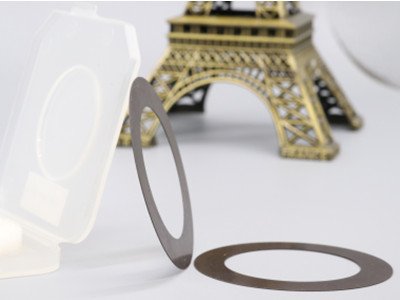
MORESUPERHARD 1A8 series resin‑bond diamond dicing blades are purpose‑engineered for singulation of QFN, DFN, BGA and LGA semiconductor packages. The resin matrix features good elasticity and self‑sharpening capability, which absorbs cutting shock, restrains micro‑crack extension and mitigates chipping, copper burr and delamination risks.
| Parameter | Recommended Setting | Remarks |
|---|---|---|
| Spindle Speed | 20 000‑30 000 rpm | Tune according to blade thickness |
| Feed Rate | 30‑70 mm/sec | Reduce feed speed for high‑density QFN to lower lateral stress |
| Coolant (pure water) | ≥ 1.5 L/min | Guarantee heat dissipation and effective flushing of cutting debris |
For QFN devices requiring wettable flank sidewalls, adopt a two‑stage step‑cut workflow. First, perform shallow pre‑cutting on the copper layer using fine‑grit MORESUPERHARD resin‑bond blade; execute full‑depth cutting in the second pass. This strategy disperses concentrated cutting stress and significantly reduces edge chipping risk.
Control spindle radial & axial run‑out within ≤ 25 µm (≤ 0.001 inch). Regular spindle maintenance and standardized blade mounting eliminate vibration‑induced cyclic chipping defects.
When MORESUPERHARD 1A8 resin‑bond dicing blades are combined with optimized cutting recipes, step‑cut procedure and tight run‑out control, manufacturers can achieve clean, burr‑free singulation edges. This solution cuts EMC chipping, copper burr and substrate delamination failure rates, lifts production yield, and improves long‑term reliability of QFN semiconductor components.

QFN chipping during dicing is a multi‑factor defect originating from blade hardware, cutting parameters, cooling condition and equipment mechanical status. Adopting purpose‑designed resin‑bond diamond dicing blades together with standardized process recipes offers a systematic mitigation path. Semiconductor packaging houses can suppress EMC chipping, copper burrs and delamination, raise manufacturing yield and enhance component reliability for QFN‑family packages.