01
Sep
With the rapid development of semiconductors, LEDs, optoelectronics and advanced electronics industries, wafer processing demands higher standards for machining accuracy, surface quality, production yield and efficiency. Sapphire wafers and silicon wafers are two core substrate materials widely adopted across chip manufacturing, LED lighting, optical communication and consumer electronics sectors. However, significant differences in their crystal properties lead to completely distinct grinding behaviors. Improper sharing of grinding wheels will cause various production issues such as chipping, severe subsurface damage, low processing efficiency and shortened wheel service life.
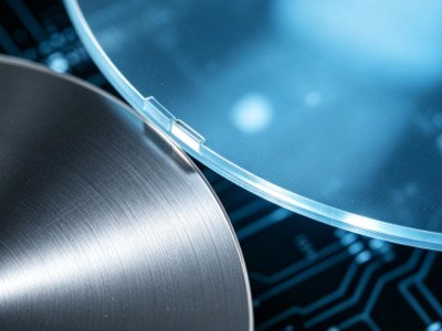
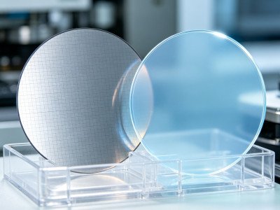
Moresuperhard specializes in grinding solutions for semiconductor hard‑and‑brittle materials. We provide customized full‑process diamond grinding wheel solutions for sapphire and silicon wafer manufacturing. Our products cover cutting, chamfering, rough grinding, fine grinding and thinning processes, and are compatible with mainstream wafer processing equipment including Speedfam and Shuwa. We help customers balance processing efficiency, finished‑product yield and wheel service life, and optimize overall production costs.
Sapphire is mainly composed of single‑crystal alumina (Al₂O₃), with a Mohs hardness of 9, second only to diamond. It features outstanding wear resistance, high‑temperature resistance, excellent chemical stability and great electrical insulation. Its extreme hardness delivers superior material performance yet creates great challenges for cutting, grinding and thinning operations.
Sapphire is widely used as GaN epitaxy LED substrate. It also serves for optical windows, laser optoelectronic devices, RF components, power electronic devices and optical parts for consumer electronics.
For sapphire pre‑process rough machining, 400‑mesh composite‑bond grinding wheels are commonly used. This bond system combines high wear resistance of metal bond and sharp cutting performance of resin bond. For grit size finer than 400#, vitrified bond wheels are preferred. After grinding, PFM physical polishing or CMP chemical mechanical polishing with diamond polishing pads can achieve surface quality at 100 nm for LED substrate requirements.
Made of high‑purity monocrystalline silicon, silicon wafer is the cornerstone of modern integrated circuits. It possesses favorable semiconductor properties with mature industrial chains and large‑scale mass production. Silicon wafers are extensively applied in GPUs, MCUs, memory chips, power devices, MEMS and various integrated circuits. Subsequent critical processes such as photolithography and thin‑film deposition heavily rely on superior surface quality of silicon wafers.
Silicon is also brittle but much softer than sapphire, resulting in relatively lower grinding difficulty. Instead of pursuing aggressive material removal, silicon wafer processing focuses on minimizing surface and subsurface damage induced by grinding.
| Comparison Item | Sapphire Wafer | Silicon Wafer |
|---|---|---|
| Main Composition | Single‑crystal Al₂O₃ (Alumina) | Single‑crystal Si |
| Material Property | Electrical insulator | Semiconductor |
| Mohs Hardness | ~9 | Significantly lower |
| Wear Resistance | Extremely high | Moderate |
| Brittleness | High | High |
| Chemical Stability | Excellent | Relatively moderate |
| Processing Difficulty | High‑hardness hard‑to‑grind, prone to chipping & cracking | Moderate difficulty; strict control over machining damage |
| Main Applications | LED substrates, optical components, RF devices | ICs, memory chips, MEMS, power devices |
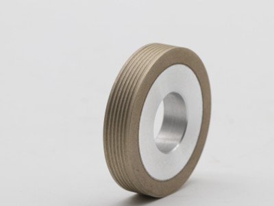
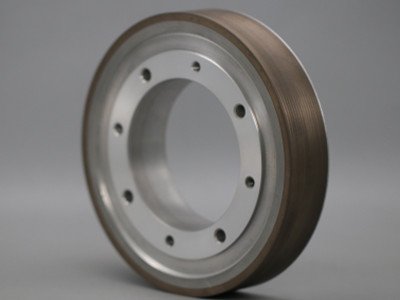
Sapphire ingot → Slicing → Squaring / OD grinding → Chamfering → Rough grinding → Thinning → Fine grinding → Lapping → Polishing → Cleaning
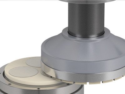
Silicon ingot → Slicing → Grinding → Chamfering → Thinning → Lapping → Polishing → Cleaning
The overall workflow resembles sapphire processing, yet priorities are different. Silicon wafer grinding focuses on TTV, flatness, surface roughness, subsurface damage and edge quality. Grinding‑induced damage will directly degrade chip yield, so low grinding force is essential for silicon wafer wheels.
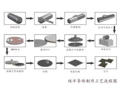
Wheel selection cannot depend merely on workpiece material. Multiple factors must be considered: wafer size, wafer thickness, material removal allowance, machine model, spindle speed, feed rate, cooling condition, production target, required surface roughness, TTV and flatness.
Recommended grit range by processing stage:
Difficulty ranking of material machining: Silicon wafer < Sapphire < SiC. As hardness rises, higher requirements are imposed on diamond abrasive quality, bond formulation, wheel self‑sharpening performance and wheel structure design. Sapphire and SiC demand far more advanced wheel development technology than ordinary silicon wafers.
Drawing on rich technical experience in hard‑and‑brittle semiconductor material grinding, Moresuperhard has developed a full portfolio of diamond grinding wheels for mass‑production sapphire and silicon wafer processing. Multiple bond systems including metal, resin, composite and vitrified bonds are available with custom formulation support for real‑world production conditions.
Our custom‑tuned wheels help manufacturers improve finished‑product yield and lower comprehensive consumable costs.
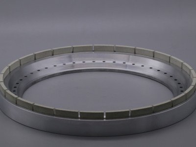
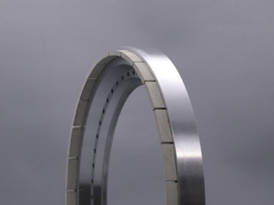
Sapphire wafers and silicon wafers are both vital semiconductor wafer materials, yet their physical properties differ greatly. Sapphire processing focuses on overcoming extreme hardness to solve chipping and efficiency challenges; silicon wafer processing prioritizes low‑stress, low‑subsurface‑damage and ultra‑high flatness. It is not recommended to reuse the same diamond grinding wheel for both materials.
Moresuperhard advises manufacturers to evaluate wheel selection comprehensively from four dimensions: material property, processing procedure, machine condition and finished‑part precision requirements, so as to achieve high‑efficiency, low‑damage and high‑yield wafer processing.
If you are facing technical challenges in sapphire or silicon wafer grinding, thinning or chamfering, please contact Moresuperhard technical team for professional wheel selection suggestions and process support.